Asynchronous FIFO: Simulation using Modelsim
Test bench strategy is to generate all corner conditions like full and empty. Simulation waveforms are shown in Figure (11) to Figure (13). These waveforms are generated using test bench program provided in previous article. Read clock frequency 50 MHz and write clock frequency 10 MHz are generated using initial procedural statements:
initial begin #10 r_clk=0; forever #10 r_clk=~r_clk; end
initial begin #5 w_clk=0; forever #50 w_clk=~w_clk; end
Duty cycle of r_clk is 10 nS and w_clk is 50 nS.
Other conditions like w_en, r_en etc are generated using below set of statements:
initial begin d_in=1;
@(posedge w_en);
repeat(20) @(posedge w_clk) d_in=d_in+2;
repeat(20) @(posedge w_clk) d_in=d_in-1;
end
initial begin reset=1;#30 reset=0;end
initial begin fork #50 w_en=1; #1800 w_en=0; #2500 w_en=1 ; join end
initial begin fork #50 r_en=0; #1850 r_en=1; #2400 r_en=0; #2500 r_en=1; join end
In the above two statements ‘fork’ and ‘join’ are used to start the simulation at zero simulation time. Reset signal is activated for first 30 nS and then it is deactivated. For the first 5 nS reset is active which tests asynchronous reset condition
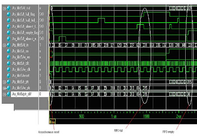
For asynchronous reset condition except d_out all other variables are initialized to default states, including f_empty_flag. r_ptr, w_ptr, ptr_diff are initialized to zero. All FIFO status flags are initialized to default values. Since reset signal is connected to binary counters, reset of counters causes reset of both read and write pointers, pointer difference and all status flags. This can be observed in the simulated waveform shown in Figure (11). Verilog code has to be improved for the complete asynchronous reset including reset of d_out. When I tried to add asynchronous reset to RTL code of dual port RAM, synthesizer does not infer dual port RAM. Instead, it infers set of registers. This problem has to be sorted out.

Figure (11) Simulation waveform 1
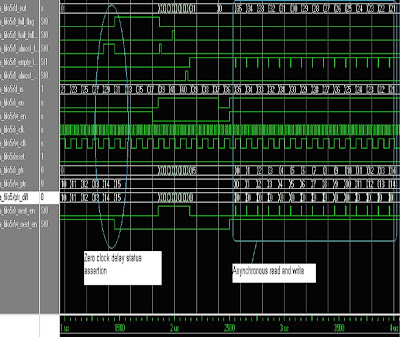
After 1800nS amount of time w_en is disabled. This time gap is chosen so that FIFO full condition can be generated. (See Figure (11)). When ptr_diff becomes equal to (fifo_depth-1) f_full_flag goes high and w_ptr stops counting. Further data on the d_in bus will overwrite on the last location of the FIFO. This is unavoidable since there is no control over the d_in bus. When FIFO is half filled (i.e. fifo_depth/2) f_half_full_flag is asserted and in next w_clk cycle it goes to normal state. Similarly when FIFO reaches almost full condition f_almost_full_flag is asserted. Thus all status flags are activated within zero clock delay. (See Figure (13))
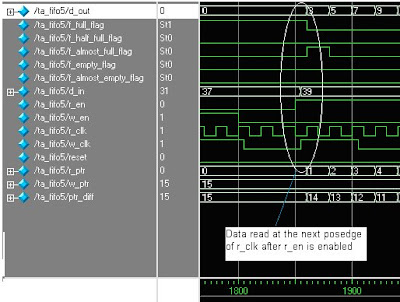
Signal r_en enabled to start read operation. At this time w_en is disabled so that empty condition can be generated. R_en is detected in coming positive edge of clock cycle and hence data is read with zero r_clk cycle delay. (See Figure (12). When ptr_diff becomes zero f_empty_flag is asserted. r_ptr stops incrementing. But for every r_clk data is read from the last location and put on to the d_out bus.

Figure (12) Simulation waveform 2
When both r_en and w_en are enabled read clock domain has to wait till data has been written to FIFO. Thus empty flag goes low for the positive edge of w_clk. At the next positive edge of the r_clk data has been read out and put in d_out bus. Since r_ptr has incremented ptr_diff becomes zero and f_empty_flag goes high again. This status remains till next positive edge of w_clk. Observe the asynchronous read and write operation in the Figure (13). F_empty_flag and r_next_en signals are compliment to each other. As soon as data is written to the FIFO r_next_en signal is enabled. Read address is incremented and both read and write pointers become equal. This makes the ptr_diff zero and once again f_empty_flag is asserted. Thus there is no pessimistic reporting of assertion or removal of FIFO status flags.
Thus overall performance of the designed FIFO resembles the performance of the FIFO IP core provided by the Xilinx. Algorithm and methodology used are entirely different in both designs. IP core uses acknowledgement signal for the confirmation of read and write operation. But proposed design does not have any such mechanism. It is assumed that data sending and receiving hardware takes care of the data once the FIFO full and empty condition are asserted.

Figure (13) Simulation waveform 3
Asynchronous FIFO: Synthesis using Xilinx ISE and Spartan 3
----------------------------------------------
Timing Summary:
Speed Grade: -5
Minimum period: 8.785ns (Maximum Frequency: 113.830MHz)
Minimum input arrival time before clock: 4.692ns
Maximum output required time after clock: 12.049ns
Maximum combinational path delay: No path found
---------------------------------------------------------
Maintaining ‘area’ as optimization goal, maximum achievable frequency is 90.212MHz.
--------------------------------------------------------
Timing Summary:
Speed Grade: -5
Minimum period: 11.085ns (Maximum Frequency: 90.212MHz)
Minimum input arrival time before clock: 4.574ns
Maximum output required time after clock: 13.375ns
Maximum combinational path delay: No path found
---------------------------------------------------------------------
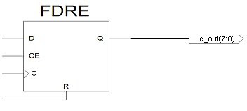
The difference in the operating frequency can be attributed to the delay in the adder-subtractor circuit. Dual port distributed RAM is used for memory. Output data d_out is registered (RTL schematic is shown in Figure (14)) which is one of the advantages of this design.

Figure (14) Registered output
The part of the synthesis report generated by Xilinx ISE, shown below infers the hardware which remains same for both optimization goals.
----------------------------------------------------------------------
Synthesizing Unit
Related source file is a_fifo5.v.
Found 16x8-bit dual-port distributed RAM for signal
-----------------------------------------------------------------------
| aspect ratio | 16-word x 8-bit | |
| clock | connected to signal
| write enable | connected to internal node | high |
| address | connected to signal
| dual address | connected to signal
| data in | connected to signal
| data out | not connected | |
| dual data out | connected to internal node | |
| ram_style | Auto | |
-----------------------------------------------------------------------
INFO:Xst:1442 - HDL ADVISOR - The RAM contents appears to be read asynchronously. A synchronous read would allow you to take advantage of available block RAM resources, for optimized device usage and improved timings. Please refer to your documentation for coding guidelines.
Found 8-bit register for signal
Found 4-bit addsub for signal <$n0003>.
Found 4-bit comparator greater for signal <$n0007> created at line 60.
Found 4-bit comparator less for signal <$n0008> created at line 62.
Found 4-bit adder for signal <$n0009> created at line 64.
Found 4 1-bit 2-to-1 multiplexers.
Summary:
inferred 1 RAM(s).
inferred 8 D-type flip-flop(s).
inferred 2 Adder/Subtracter(s).
inferred 2 Comparator(s).
inferred 4 Multiplexer(s).
Unit
-----------------------------------------------------------------
But observation of the low level synthesis gives the device utilization summary. Device utilization with ‘speed’ as optimization goal is as follows:
-----------------------------------------
Device utilization summary:
---------------------------
Selected Device: 3s200ft256-5
Number of Slices: 36 out of 1920 1%
Number of Slice Flip Flops: 20 out of 3840 0%
Number of 4 input LUTs: 50 out of 3840 1%
Number of bonded IOBs: 24 out of 173 13%
Number of GCLKs: 2 out of 8 25%
-------------------------------------------------------------
Device utilization with ‘area’ as optimization goal is as follows:
-----------------------------------------
Device utilization summary:
-----------------------------------------
Selected Device : 3s200ft256-5
Number of Slices: 34 out of 1920 1%
Number of Slice Flip Flops: 16 out of 3840 0%
Number of 4 input LUTs: 47 out of 3840 1%
Number of bonded IOBs: 24 out of 173 13%
Number of GCLKs: 2 out of 8 25%
------------------------------------------------------------
Related Articles
-
Asynchronous FIFO Design
-
FIFO Pointers
Verilog code for asynchronous FIFO
-
Verilog Test Bench for Asynchronous FIFO
-
New Asynchronous FIFO Design
Asynchronous FIFO-Clock Generation Using DCM
No comments:
Post a Comment
Your Comments... (comments are moderated)